
Prototyping
Turning advanced technology concepts into tangible demonstrators, functional samples, evaluation structures and proof-of-concept devices. NT&D supports the realization of physical prototypes for projects involving nanotechnology, advanced materials, micro- and nanoscale fabrication, functional surfaces and device-oriented innovation. This approach helps transform scientific and technical ideas into measurable structures that can be evaluated, refined and communicated as part of the path toward further development, collaboration or technology transfer.
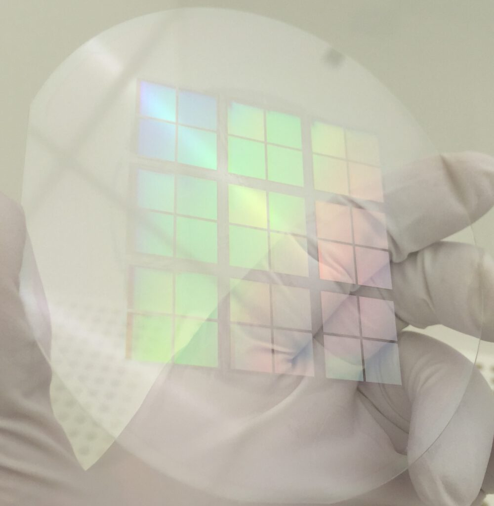
From technical concept to tangible demonstrator
Advanced concepts often need a physical implementation before their technical potential can be properly assessed. A material property, process route, surface function or device idea may look promising in theory or during early R&D, but meaningful progress usually requires a demonstrator that can be fabricated, handled, measured and improved.
Realization may involve micro- and nanoscale structuring, thin-film processing, surface preparation, metallization, pattern transfer, nanoimprint-based workflows, device integration or the fabrication of dedicated evaluation structures. The objective is not always a final product, but a technically meaningful sample or device that helps answer concrete development questions.
Prototype formats can range from individual evaluation samples and small experimental layouts to wafer-scale demonstrators on substrates up to 200 mm. This flexibility allows the prototype format to match the technical goal of the project, whether the focus is feasibility, functionality, integration, performance evaluation or preparation for the next development stage.
Fabrication, integration and evaluation
The realization of functional demonstrators connects technical feasibility with practical evidence. A well-designed prototype provides more than a visual representation of an idea; it creates a physical basis for evaluating function, manufacturability, integration behavior, material compatibility and application relevance.
NT&D combines process know-how, device-oriented thinking and interdisciplinary R&D experience to support prototype realization across materials, surfaces, structures and fabrication workflows. This includes selecting suitable process routes, defining evaluation structures, considering integration requirements and aligning the physical implementation with the technical questions that need to be answered.
Depending on the project, the result may be a proof-of-principle device, a structured sample, a functional evaluation vehicle, a wafer-level demonstrator, a process demonstrator or an early device concept. These outputs can support internal development, partner discussions, technical validation, collaboration preparation or transition toward technology transfer.
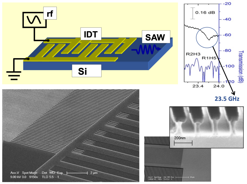
SAW devices for piezoelectric generation of ultrahigh-frequency surface acoustic waves on silicon substrates. Interdigital transducers (IDTs) are fabricated using CMOS-compatible processes on a ZnO piezoelectric layer embedded between two SiO₂ layers on top of a silicon substrate. Electrode features with 65 nm dimensions enable acoustic modes up to 23.5 GHz. At the device level, the multilayer concept is suitable for acoustic charge transport and advanced signal processing on integrated silicon-based technology platforms at extremely high frequencies, with only moderate carrier mobility requirements.
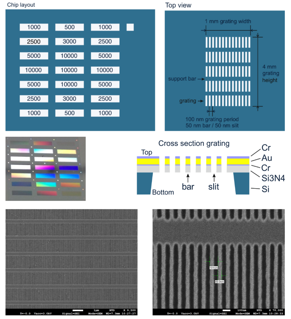
Freestanding transmission gratings for optical and spectroscopic applications from the visible to the EUV range. The chip contains a 3 × 7 array of grating structures on a 21 mm × 17 mm substrate, with individual grating areas of 4 mm × 1 mm. High-density gratings up to 10,000 lines/mm are realized, corresponding to a 100 nm grating period with 50 nm bars and 50 nm slits. The multilayer membrane concept is relevant for advanced spectroscopy, optical components, nanoscale structuring and application-specific photonic demonstrators.
Application-specific demonstrators
Prototype realization is strongly shaped by the intended application. The required materials, dimensions, process flows, functional layers, interfaces and evaluation methods differ significantly between electronics, photonics, biotechnology, MEMS/NEMS, molecular-scale concepts, metamaterials and advanced process technologies.
NT&D supports demonstrator and evaluation-structure fabrication across advanced technology fields where nanoscale materials, micro- and nanoscale fabrication, functional surfaces and device concepts intersect. In interdisciplinary projects, these areas can also be combined to create physical samples or device-oriented structures that connect materials, processes, architectures and functions within one coherent technical route.
Micro- and Nanoelectronic Devices
Micro- and nanoelectronic device prototypes can include complete device structures, electrode layouts, contact architectures, interconnect patterns, thin-film stacks, sensor elements, SAWs, transistor-like structures, diode structures and patterned functional layers. These prototypes help evaluate how material choice, interface quality, geometry, metallization and fabrication sequence influence electrical behavior and device functionality.
Prototype realization in this area provides a practical basis for measurement, comparison and design refinement. By moving from individual structures toward complete device formats, key technical questions can be evaluated more clearly and suitable fabrication routes for advanced electronic platforms can be defined with greater confidence.
Graphene & 2D Material Structures
Graphene and 2D material structures can include patterned graphene layouts, graphene field-effect device concepts, contact structures, transfer-based samples, hybrid material stacks, sensing layouts, photodetector-oriented structures and functionalized surfaces. These prototypes help assess how atomically thin materials behave when integrated with electrodes, substrates, dielectrics, optical structures or other device elements.
Realization in this area makes it possible to evaluate contact behavior, interface quality, pattern fidelity, processing compatibility and the relationship between material quality and device function. Structured graphene and 2D material samples can support refinement of sensing, electronic, optoelectronic or surface-based concepts before moving toward more complete device formats.
Molecular-scale Architectures
Molecular-scale architectures can include nanogap electrode structures, nanoscale junction layouts, functionalized surfaces, molecular interface structures, electrode–molecule–electrode configurations and device-oriented layouts for investigating molecular interactions or charge transport. These structures make nanoscale and molecular effects accessible to controlled measurement and technical evaluation.
Prototype realization in this field provides an experimental bridge between molecular functionality and device-level behavior. Carefully designed architectures can support the evaluation of coupling mechanisms, interface stability, surface chemistry, electrode geometry and integration routes for molecular-scale technology concepts.
Optical & Photonic Components
Optical and photonic components can include waveguides, gratings, resonators, diffractive optical elements, photonic crystal structures, micro-optical surfaces, integrated optical layouts, photodetector-related structures and functional thin-film components. These prototypes help evaluate light guidance, coupling, diffraction, reflection, transmission, absorption or light–matter interaction in structured materials and device geometries.
Physical realization allows parameters such as pattern fidelity, surface quality, optical coupling, material selection and integration with other device elements to be assessed directly. The resulting components can support performance evaluation, design refinement and communication of photonic, optoelectronic or integrated-optics concepts.
Biotechnology & Medical Device Concepts
Bio- and medical device concepts can include microfluidic chips, lab-on-chip structures, structured biosensor surfaces, sensing-electrode layouts, fluidic channels, microstructured interfaces, functional coatings and device-oriented samples for interaction with biological or chemical environments. These prototypes support the evaluation of fluid handling, surface functionality, detection principles and integration with optical or electronic readout concepts.
Realization in this area helps connect advanced materials and microfabricated structures with application-specific requirements such as sample handling, interface behavior, biocompatibility considerations, sensing geometry and practical device configuration. The resulting samples can provide a physical basis for evaluating bio- and medical technology concepts before further refinement or collaboration.
MEMS & NEMS Systems
MEMS and NEMS prototypes can include micro- and nanoscale mechanical structures, resonators, cantilevers, membranes, suspended features, sensor elements, actuator structures, micromirrors, contact layouts and integrated electromechanical device samples. These systems help evaluate how geometry, material properties, layer stacks, release steps and interfaces influence mechanical or electromechanical behavior.
Realization of MEMS and NEMS structures requires careful attention to fabrication sequence, structural stability, packaging considerations and integration with electrical, optical or fluidic functions. The resulting devices or prototype structures can provide essential feedback for refining miniaturized systems, high-end sensor concepts and actuator-based technologies.
Metamaterials & Functional Structures
Metamaterials and functional structures can include metasurfaces, periodic micro- and nanostructures, plasmonic arrays, engineered surface patterns, diffractive structures, resonant geometries, functional textures and nanoimprint-based architectures. These prototypes make it possible to evaluate how controlled geometry, periodicity, material composition and feature dimensions influence optical, electronic, mechanical or surface-related behavior.
Physical samples help connect design intent with measurable response. By fabricating defined structures and evaluating their behavior, structure–function relationships can be assessed, design assumptions can be refined and application-specific performance targets can be explored for optics, sensing, surface engineering or other advanced technology concepts.
Materials & Process Samples
Materials and process samples can include thin-film stacks, coated substrates, functional surfaces, patterned layers, metallized substrates, lift-off structures, etched features, multilayer samples, contact metallization, nanoimprinted surfaces and sample-to-wafer process flows. These samples help evaluate how materials, surfaces and fabrication steps behave under practical fabrication conditions.
Such samples can support comparison of process routes, assessment of functional layers, evaluation of reproducibility and refinement of integration strategies. The goal is to create reliable technical evidence that a material system, surface treatment or fabrication approach can support further realization toward application-oriented implementation.
See how prototyping connects with NT&D’s consulting, R&D and technology transfer services.
Discuss your prototyping challenge
Contact NT&D to explore how functional demonstrators, evaluation structures, proof-of-concept devices and prototype fabrication can support your advanced technology project.