
Gratings and Diffractive Micro- and Nanostructures
NT&D develops and fabricates application-specific gratings and diffractive micro- and nanostructures for optical, spectroscopic and photonic applications. The focus is on translating demanding optical concepts into realistic micro- and nanofabrication approaches, including high-density grating structures, membrane-based devices, transmission and reflection gratings, diffractive mirrors and customized optical demonstrators.
These structures can support applications where optical function depends on precisely defined periodic patterns, material stacks, membrane geometries, surface quality and process integration. Depending on the requirements, grating concepts can be developed for transmission or reflection, visible to ultraviolet and EUV-related applications, spectroscopy, beam control, optical filtering, diffractive optics, photonic components and application-specific research devices.
Freestanding transmission gratings
Freestanding transmission gratings are membrane-based optical components in which nanoscale grating structures are fabricated in a thin functional membrane. They are relevant for optical and spectroscopic applications where transmitted light interacts with precisely defined periodic structures. Compared with conventional supported structures, freestanding membrane concepts can provide optical access through open slit areas while maintaining mechanical stability through a designed support layout.
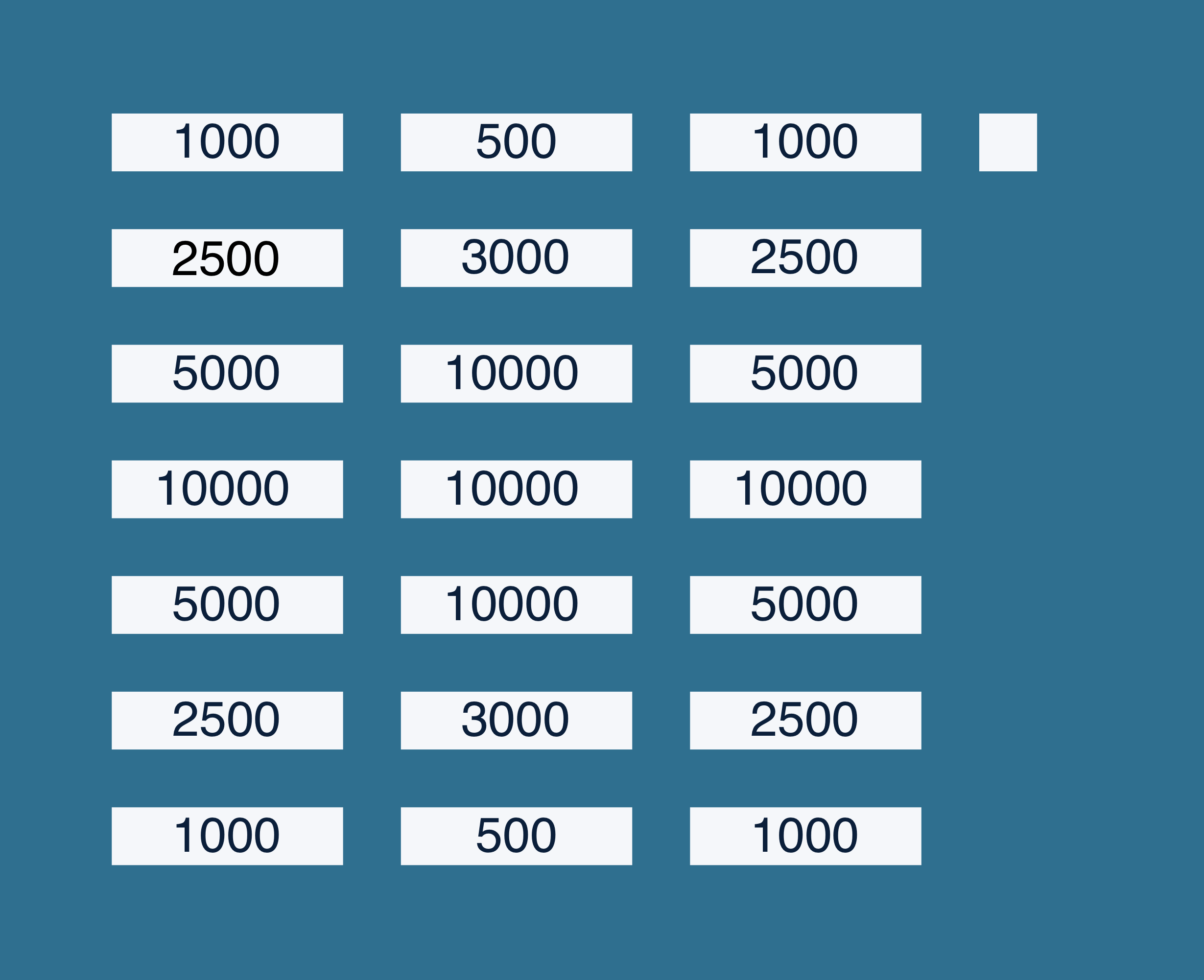
NT&D has developed freestanding transmission grating chips with multiple grating areas on one substrate. A representative chip contains 21 individual gratings arranged in a 3 × 7 array on a 21 mm × 17 mm chip. Each grating area has a size of 4 mm × 1 mm, allowing different grating periods to be integrated, compared and evaluated on one compact device platform.
The demonstrated grating periods cover a broad range from 500 to 10,000 lines/mm. The highest-density structures correspond to a 100 nm grating period with 50 nm bars and 50 nm slits, placing these features clearly in the nanoscale range. This makes the concept suitable for demanding optical and spectroscopic applications from the visible range toward ultraviolet and EUV-related use cases.
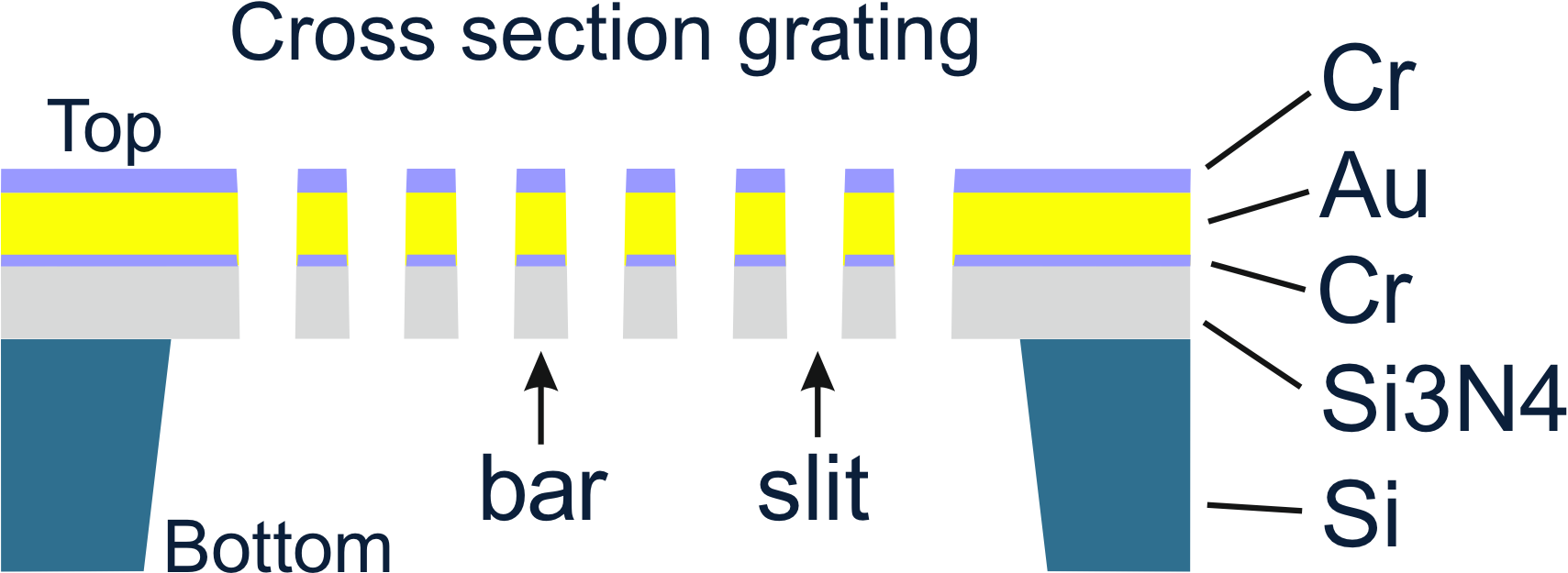
The membrane concept can be realized using a 200 nm Si₃N₄ membrane with a 60 nm gold layer on top. Other metal layers, membrane materials or layer stacks can be considered depending on the optical, mechanical and fabrication requirements of the intended application. Optional reference membrane windows with variable size and position can also be included to support comparison measurements, optical reference areas or application-specific evaluation.
Chip layout
Top view single grating
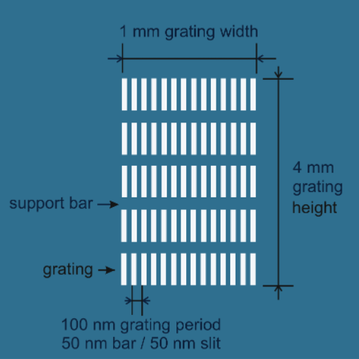
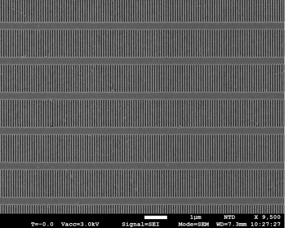
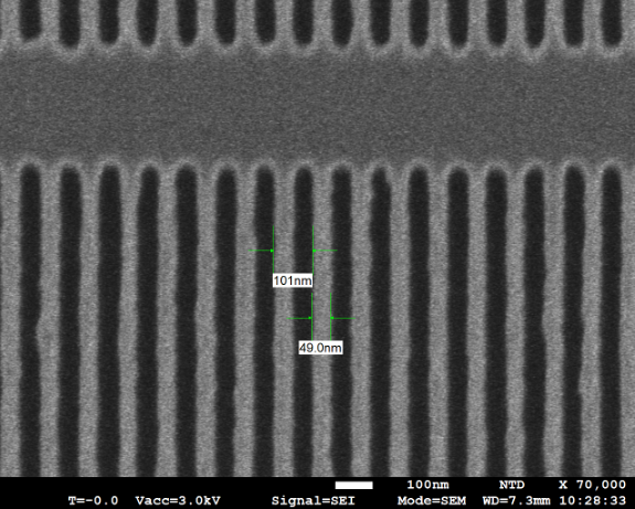
Typical design parameters include grating period, line width, slit width, grating area, support bar width, support bar period, membrane thickness, metal layer stack, chip size, window layout and substrate format. These parameters must be considered together because optical performance, mechanical stability and fabrication feasibility are strongly connected in freestanding grating devices.
Representative grating specifications include:
These specifications can be adapted for application-specific layouts, optical requirements, material systems and demonstrator concepts.
Application-specific grating and diffractive structure development
In addition to freestanding transmission gratings, NT&D can support the development and fabrication of other grating-based and diffractive micro- and nanostructures. This may include reflection gratings, diffractive mirrors, structured optical surfaces, nanoscale periodic patterns, photonic test structures, diffractive optical elements and application-specific optical demonstrators.
This development approach connects grating design with device-oriented prototyping and advanced nanofabrication processes, supporting the transition from optical or spectroscopic requirements toward realistic fabrication routes. This is especially important for high-density grating structures, membrane-based devices and diffractive components where geometry, material properties, mechanical stability and process compatibility must be considered together.
Different grating concepts can be designed and fabricated on different material bases, depending on the optical function and integration requirements. Possible approaches may involve metallic, dielectric, semiconductor, membrane-based, thin-film or multilayer structures. Reflection gratings and diffractive mirrors may require different layer stacks, surface properties, pattern depths, material contrasts and process sequences compared with freestanding transmission gratings.
The fabrication route can include high-resolution lithography, nanoimprint lithography, thin-film deposition, metallization, lift-off, etching, membrane processing, surface preparation and process integration. The choice of process depends on the required grating period, feature size, optical wavelength range, substrate material, layer stack, aspect ratio, mechanical stability and final device function.
This flexibility makes it possible to evaluate customized grating geometries and diffractive designs for spectroscopy, optical components, beam shaping, wavelength-selective elements, photonic systems, sensor-related applications and research-oriented optical devices. NT&D can support projects from early feasibility assessment and layout discussion to fabrication route development, prototype realization and device-oriented evaluation.
Discuss your grating or diffractive optics challenge
Contact NT&D to discuss freestanding transmission gratings, reflection gratings, diffractive mirrors or application-specific diffractive micro- and nanostructures for optical, spectroscopic and photonic applications.