
Advanced Technologies
Enabling technologies and process capabilities for the development of advanced materials, functional structures and device-oriented solutions. NT&D combines process know-how, interdisciplinary R&D experience and practical implementation expertise to support complex high-tech concepts from early feasibility assessment toward functional realization.
Advanced cleanroom and laboratory infrastructure
Advanced cleanroom and laboratory infrastructure is a key foundation for nanofabrication and the practical realization of high-tech materials, structures and device concepts.. NT&D combines its process know-how, developed technologies and interdisciplinary R&D expertise with established access to advanced cleanroom, nanofabrication and laboratory environments, including MESA+ NanoLab at the University of Twente and Nanolab AMICA at AMO GmbH.
This infrastructure supports high-end technologies for micro- and nanoscale fabrication, including high-resolution lithography, nanoimprint lithography, thin-film deposition, metallization, etching, surface preparation, characterization and related cleanroom-based workflows. It enables advanced concepts to be evaluated, fabricated and refined under professional conditions required for device-oriented development and technology implementation.
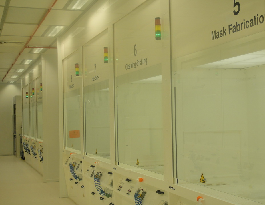
The available cleanroom and laboratory infrastructure provides a state-of-the-art environment for advanced micro- and nanotechnology development. This includes cleanroom facilities up to ISO 5 / ISO 7 with approximately 1250 m² of controlled fabrication space, complemented by specialized analysis areas and dedicated research laboratories for high-resolution imaging, surface and bulk analysis, material evaluation and device-oriented investigation. Additional highly flexible cleanroom capabilities in the class 10 to 1000 range support nanometer-scale lithography, pattern transfer, deposition, etching, wet chemistry and characterization workflows.
Together, this infrastructure provides a powerful foundation for high-quality and precise work across demanding fabrication, structuring and development tasks. It supports lithography, nanoimprint, thin-film processing, metallization, micro- and nanostructuring, surface preparation, interface control, process integration and device evaluation under professional cleanroom and laboratory conditions. By combining advanced infrastructure with established process know-how and interdisciplinary R&D expertise, NT&D can support complex projects that require controlled process conditions, reliable fabrication routes, accurate characterization and the practical translation of advanced concepts into functional technology solutions.
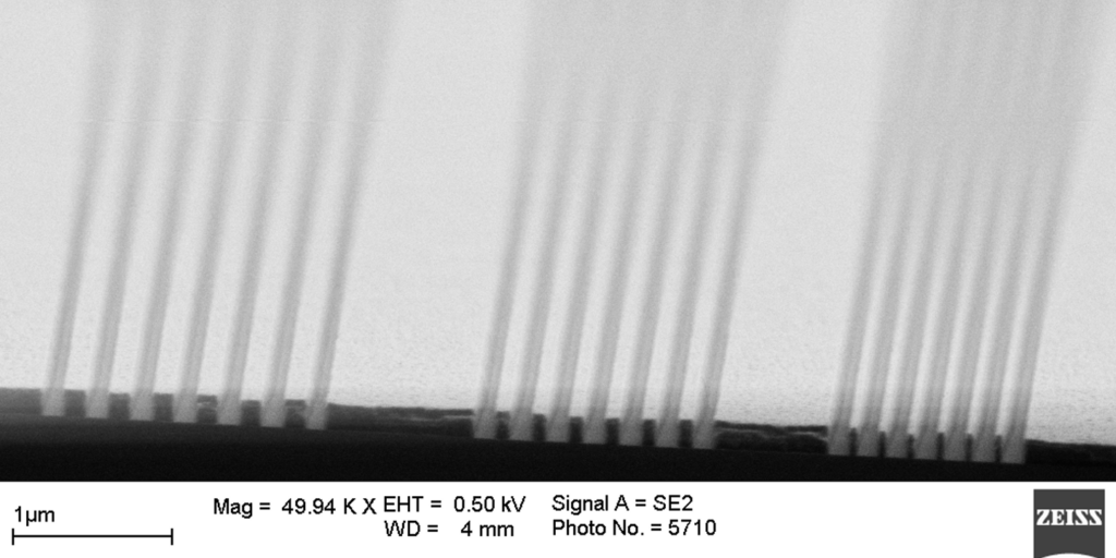
Enabling technologies and process capabilities
Advanced technologies and process capabilities form the technical foundation for transforming materials, surfaces and device concepts into functional high-tech solutions. NT&D combines more than 30 years of nanotechnology experience with established process know-how, developed technologies and interdisciplinary R&D expertise across micro- and nanoscale fabrication, structuring, integration and device-oriented development. This includes technology development, prototyping and process development from small samples to wafer-scale processing on substrates up to 200 mm, supporting the evaluation, refinement and realization of advanced concepts for next-generation technology platforms.
Pattern Definition & High-Resolution Lithography
Pattern definition is a central step in micro- and nanotechnology, enabling the controlled transfer of designs into resists, functional layers and device-oriented process flows. Modern lithography includes a broad range of methods, from optical approaches used for reproducible microfabrication to high-resolution direct-write techniques for nanoscale research and development.
Capabilities in this area may involve mask aligner lithography, stepper-based projection lithography, contact and proximity exposure, laser lithography, interference lithography, grayscale exposure concepts, electron-beam lithography and related direct-write approaches. The choice of method depends on resolution, area, alignment accuracy, substrate format, material compatibility and the intended function of the final structure.
This field connects design, resist processing, alignment, exposure, development and downstream pattern transfer. It supports applications ranging from microelectronic and photonic structures to sensors, microfluidics, functional surfaces and exploratory nanoscale device architectures.
Nanoimprint Lithography
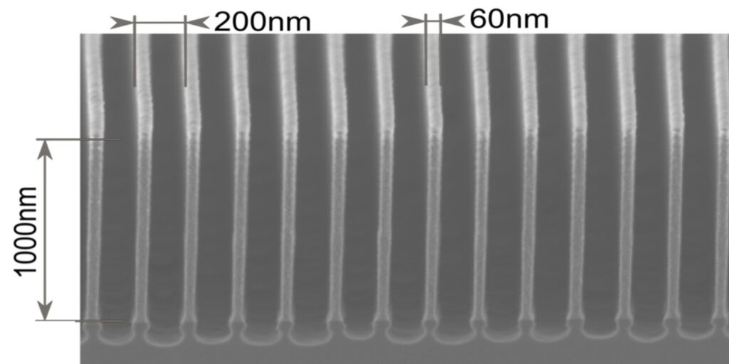
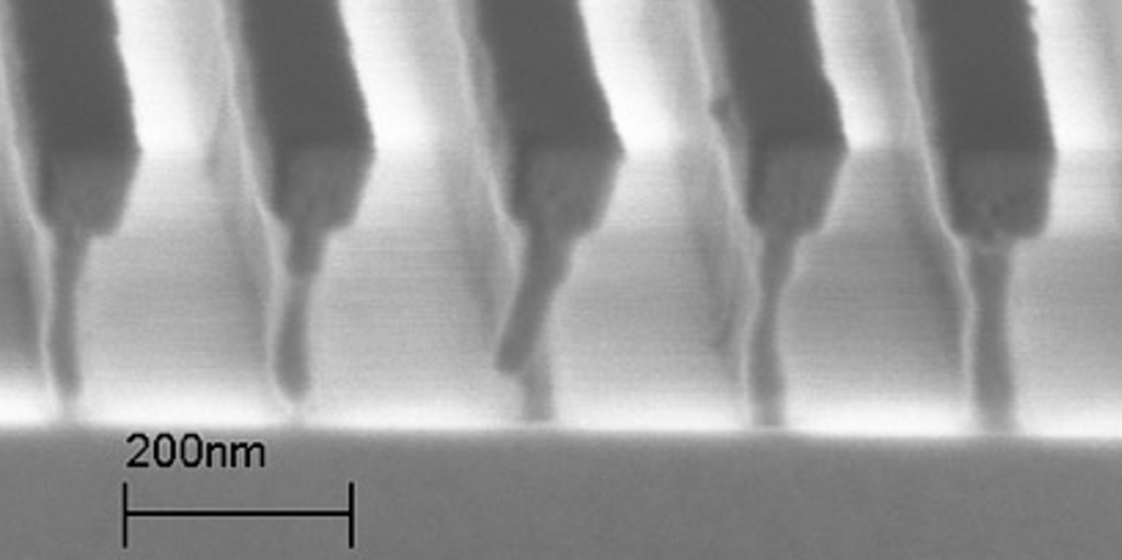
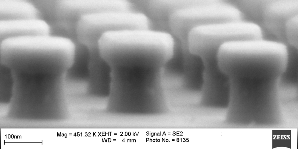
Nanoimprint lithography is a key technology for high-resolution replication of micro- and nanoscale structures. In contrast to purely optical exposure methods, NIL transfers topography from a structured template into a moldable material, enabling dense nanoscale features, high pattern fidelity and scalable replication concepts.
NT&D has deep expertise in nanoimprint-related technologies, including process concepts for UV nanoimprint, thermal nanoimprint, stamp and mold considerations, residual-layer control, pattern replication, functional nanostructures and integration into broader process flows. Nanoimprint is especially relevant where high-resolution patterning must be combined with practical scalability, cost-aware fabrication or large-area structuring.
Relevant directions include nanophotonics, optical structures, gratings, metasurfaces, micro- and nanofluidic structures, functional surfaces, sensor platforms, biointerfaces, advanced polymer structures and replication-based fabrication routes for next-generation device concepts.
3D Lithography & Direct Laser Writing
3D lithography extends micro- and nanofabrication beyond planar patterning by enabling complex three-dimensional structures with controlled geometry, material distribution and functional design. Techniques such as two-photon polymerization, multiphoton lithography and direct laser writing allow the fabrication of micro- and nanoscale architectures that are difficult or impossible to realize with conventional planar lithography alone.
This field is relevant for micro-optics, photonic structures, metamaterials, biomedical scaffolds, microfluidic components, micro-robotic elements, mechanical microstructures and complex functional prototypes. It enables design freedom in three dimensions while still requiring careful consideration of materials, exposure strategy, writing resolution, surface quality, shrinkage, mechanical stability and integration with other process steps.
For NT&D, 3D lithography belongs to the broader capability base for advanced device concepts, bridging design, materials, fabrication and function. It is particularly valuable where next-generation applications require freeform structures, hierarchical geometries or complex micro-/nanoscale functionality.
Deposition & Thin-Film Technologies
Deposition technologies are essential for forming functional layers, coatings, thin films and material stacks used in advanced devices. The properties of deposited films — including thickness, uniformity, density, roughness, composition, crystallinity, interface quality and conformality – can strongly influence device performance and process feasibility.
Capabilities in this field include physical vapor deposition and chemical vapor deposition approaches such as thermal evaporation, electron-beam evaporation, sputtering, magnetron sputtering, reactive sputtering, pulsed laser deposition, thermal CVD, LPCVD, PECVD, MOCVD, ALD and plasma-enhanced ALD, as well as solution-based or hybrid coating approaches where appropriate. Different techniques are selected depending on material type, substrate requirements, layer thickness, step coverage, thermal budget and integration constraints.
This area supports the development of dielectric layers, conductive films, semiconductor materials, optical coatings, barrier layers, adhesion layers, functional surfaces, nanostructured films and multilayer stacks for microelectronics, photonics, sensors, biomedical devices and other high-tech applications.
Metallization & Contact Fabrication
Metallization and contact fabrication provide conductive layers, contact structures, interconnects, electrodes and functional metal patterns for advanced device platforms.
Capabilities in this area may include electron-beam evaporation, thermal evaporation, sputtering, magnetron sputtering, reactive sputtering, multilayer metallization, adhesion layers, seed layers, lift-off-compatible metal stacks and metal patterning for electrodes, contacts and interconnects. Material choices may include noble metals, transition metals, transparent conductive materials and application-specific multilayer systems.
This field is relevant for sensors, micro- and nanoelectronics, photonic devices, MEMS/NEMS, bioelectronic interfaces, thin-film components, test structures and device prototypes. It connects materials selection with pattern definition, process compatibility and the electrical or functional requirements of the final device.
Pattern Transfer: Etching, Lift-Off & Structuring
Pattern transfer converts a defined resist or mask pattern into a functional material structure. This step is critical because the final geometry, sidewall profile, surface quality, line-edge fidelity and material selectivity often determine whether a device concept can be realized in practice.
Capabilities in this area include wet chemical etching, dry etching, plasma etching, reactive ion etching, ICP-RIE, ion milling, atomic-layer-etching-related concepts, lift-off processes and combined subtractive/additive structuring routes. Pattern transfer also includes the careful selection of hard masks, resists, adhesion layers, etch chemistries and process sequences to achieve the required geometry and material behavior.
This field supports the fabrication of micro- and nanostructures, trenches, openings, electrodes, gratings, photonic structures, sensor elements, functional surfaces, MEMS/NEMS components and device-oriented test structures. It is one of the key bridges between pattern definition and functional implementation.
Surface Functionalization & Interface Engineering
Surface functionalization modifies material surfaces to control chemical, physical, biological, optical or interfacial behavior. In advanced device development, surfaces are often as important as the bulk material, because adhesion, wettability, biocompatibility, sensing response, contamination, bonding, passivation and molecular interaction are governed by surface and interface properties.
Capabilities in this field may include plasma activation, chemical surface modification, silanization, self-assembled monolayers, polymer coatings, hydrophilic or hydrophobic surface control, biofunctionalization concepts, adhesion promotion, passivation, cleaning strategies and interface preparation for bonding, deposition or device operation.
This area is particularly relevant for biointerfaces, microfluidics, biosensors, medical device-related concepts, functional surfaces, nanomaterial integration, optical structures and hybrid devices. It enables the adaptation of advanced materials and surfaces to the specific requirements of their intended application environment.
Process Integration, Characterization & Evaluation
Advanced technologies become useful only when individual processes can be integrated into coherent and reliable fabrication sequences. Process integration connects pattern definition, deposition, metallization, pattern transfer, surface modification, cleaning, alignment, thermal budgets, material compatibility and device requirements into practical development flows.
Capabilities in this area include process sequence design, compatibility assessment, failure analysis, test-structure planning, material and interface evaluation, optical and electrical assessment, surface and topography analysis, microscopy-based inspection, profilometry, ellipsometry, contact-angle evaluation, spectroscopic methods and interpretation of experimental results in relation to device function.
This field is essential for turning isolated process steps into functional technology platforms. It supports feasibility assessment, process optimization, troubleshooting, validation of fabricated structures and the transition from scientific concepts toward device-oriented implementation.
Discuss your technology challenge
Contact NT&D to discuss how advanced process capabilities and device-oriented development expertise can support your research, prototyping or innovation goals.