
Application and Technology Fields
Application-oriented technology fields where nanoscale materials, advanced processes and functional devices converge. NT&D combines established know-how, developed technologies and interdisciplinary R&D experience to address complex high-tech challenges from early concepts to device-oriented implementation.
Fields of expertise
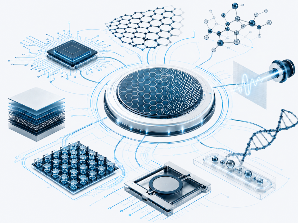
The following fields highlight selected areas where NT&D applies its expertise across materials, processes, devices and application-oriented technology development. These areas are closely connected and often overlap in interdisciplinary projects, where scientific concepts, fabrication routes, functional structures and device requirements must be considered together. The focus is on combining broad technological understanding with practical development experience to support advanced concepts from early feasibility assessment toward device-oriented implementation.
Micro- and Nanoelectronics
Micro- and nanoelectronics remain central to the development of advanced electronic systems with increased functionality, reduced dimensions and new device architectures. Current progress in this field is no longer driven only by lateral scaling, but also by heterogeneous integration, advanced materials, interface engineering, 3D integration concepts and the combination of electronic, photonic, sensing and system-level functionality.
NT&D supports technology concepts involving micro- and nanoscale electronic structures, functional layers, advanced interfaces and device-oriented architectures. This includes evaluation of material and process options, feasibility assessment of emerging device concepts, integration-related considerations and the connection between scientific principles and practical implementation routes.
The expertise is relevant for advanced electronic platforms, nanoscale functional elements, sensor-related electronics, device miniaturization, material-enabled electronics, hybrid integration concepts and early-stage approaches beyond conventional device scaling.
Graphene & 2D Materials
Graphene and related two-dimensional materials have developed into a broad technology platform for electronics, photonics, sensing, flexible systems and multifunctional devices. Their atomic-scale thickness, high surface sensitivity and distinctive electrical, optical, thermal and mechanical properties make them highly relevant for applications where conventional material systems reach practical or functional limits.
Expertise in this area supports the evaluation of graphene and 2D material concepts, the identification of suitable device routes and the integration of these materials with functional surfaces, process flows and micro-/nanoscale structures. Particular attention is given to the transition from attractive material properties toward usable technology concepts, where reproducibility, interfaces, contacts, processing conditions and integration compatibility are often decisive.
Relevant directions include graphene-based and 2D-material-enabled sensors, optoelectronic concepts, functional surfaces, hybrid material systems, miniaturized devices, flexible or conformable platforms and exploratory approaches for future electronic and photonic applications.
Molecular-scale Applications
Molecular-scale applications use molecular structures, interfaces and mechanisms as functional elements in advanced technology concepts. At these dimensions, device behavior may be influenced by charge transport, tunneling, switching, recognition effects, self-assembled layers, molecular organization or interface-controlled mechanisms that are not accessible through conventional microdevice approaches alone.
Activities in this field connect molecular functionality with materials, surfaces, nanostructures and device-oriented architectures. This includes assessing how molecular mechanisms can contribute to sensing, switching, electronic response, surface functionality or advanced material behavior, while considering the practical challenges of stability, reproducibility, contacting, integration and measurement.
Relevant directions include molecular electronics, molecular interfaces, functional molecular layers, nanoscale charge transport, recognition-based concepts, molecular sensing, self-assembled systems and hybrid approaches that combine bottom-up molecular functionality with top-down micro- and nanofabrication.
Optics & Photonics
Optics and photonics are increasingly important for high-tech systems involving light generation, manipulation, transmission, detection and integration. Current developments include integrated photonics, nano-optoelectronics, miniaturized optical sensors, metasurfaces, compact spectroscopic systems and hybrid platforms that combine optical functionality with electronic, material and micro-/nanostructured device concepts.
Application-oriented work in this area addresses optical, photonic and nano-optoelectronic systems, with attention to the interaction between materials, surfaces, geometry, fabrication processes and device-level optical performance. This includes concepts where nanoscale structures, functional layers or integrated architectures are used to influence light–matter interaction, sensing response, optical coupling or miniaturized device functionality.
Relevant directions include integrated optics, nano-optoelectronics, photonic structures, optical sensing, miniaturized optical devices, functional surfaces, light–matter interaction, photonic materials, optical diagnostics and advanced device concepts at the interface of electronics and photonics.
Biotechnology & Medical Applications
Biotechnology and medical applications increasingly rely on advanced materials, microfluidics, biosensing, miniaturized analytical systems and functional interfaces. Current developments in lab-on-chip and diagnostic platforms emphasize portability, real-time analysis, multi-analyte detection, integration of sample handling and, increasingly, data-driven or AI-assisted interpretation of measurement results.
Technology development in this area connects biointerfaces, microfluidic concepts, diagnostics, biomedical sensing, medical device-related innovation and application-oriented platforms. The focus is on linking materials, surfaces, processes and device architectures with the practical requirements of bio- and medical environments, where performance, reliability, biocompatibility, manufacturability and usability must be considered together.
Relevant directions include biointerfaces, lab-on-chip concepts, microfluidics, diagnostic platforms, biosensing, biomedical devices, functional surfaces, miniaturized analytical systems, medical-device-related technology concepts and advanced platforms for point-of-care or research-oriented applications.
MEMS & NEMS
MEMS and NEMS technologies enable micro- and nanoscale electromechanical systems for sensing, actuation, signal transduction and functional device operation. The field continues to advance through improved structural designs, new sensitive materials, refined fabrication and packaging approaches, integration with electronics and the development of high-performance sensors and actuators for demanding applications.
Concept development in this field covers high-end sensors, actuators, electromechanical devices and functional micro-/nanosystems from early ideas to device-oriented development. This includes consideration of materials, interfaces, mechanical and electrical behavior, fabrication constraints, packaging-related aspects and the requirements needed to move from a concept toward functional and system-relevant implementation.
Relevant directions include microsensors, nanosensors, actuators, resonant systems, pressure and inertial sensing concepts, functional micro- and nanostructures, electromechanical transduction, device integration, advanced sensing principles and miniaturized systems for industrial, biomedical or high-tech applications.
Metamaterials & Functional Structures
Metamaterials, metasurfaces and functional structures are designed to achieve tailored optical, electronic, mechanical or multifunctional behavior through engineered geometry, material composition or structural organization. The field has evolved from fundamental demonstrations toward application-driven platforms for photonics, sensing, imaging, communications, energy-related systems and advanced electromagnetic or mechanical functionality.
Development and evaluation in this area focus on advanced material and structural concepts where performance is defined not only by the base material, but also by patterning, dimensional control, surface design and integration. This includes concepts based on periodic or hierarchical structures, engineered surfaces, miniaturized functional elements and device-oriented approaches that require precise control of geometry, materials and fabrication routes.
Relevant directions include optical metamaterials, metasurfaces, functional surfaces, engineered micro-/nanostructures, tailored material responses, multifunctional structures, advanced patterning concepts, photonic and electromagnetic structures and device platforms based on designed structural behavior.
Advanced Materials & Processes
Advanced materials and processes form the foundation for many high-tech device concepts. Material selection, thin-film growth, deposition conditions, surface preparation, patterning, structuring, metallization, integration and process compatibility can strongly influence whether a scientific idea can become a functional and reliable device-oriented technology.
Process-oriented work in this area connects materials, surfaces, functional layers, micro- and nanostructures and fabrication routes relevant to advanced device development. This field links material understanding with process design, device requirements and application-oriented implementation, especially in projects where the performance of a technology depends on the interaction between materials, interfaces and processing steps.
Relevant directions include functional materials, thin films, nanostructured surfaces, coatings, deposition, lithography-related patterning, metallization, etching, process integration, material compatibility, surface functionality and the translation of material and process concepts into advanced device-oriented technologies.
Discuss your application challenge
Contact NT&D to discuss how expertise across advanced application fields can support your research, development or innovation goals.